

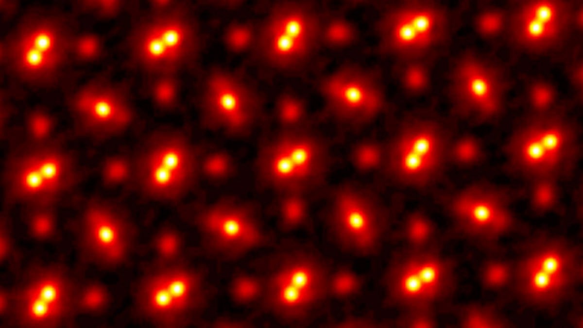
They say it’s a picture of atoms, but what are the atoms: the glowing yellow balls or the entire meatball including the darker red? If it’s the meatballs, then why do some have apparently two nuclei?
Here’s the public press release: https://news.cornell.edu/stories/2021/05/cornell-researchers-see-atoms-record-resolution
Here’s the actual scientific article: https://www.science.org/doi/10.1126/science.abg2533
That is only sort of true - this image is not made of electrons reflected by the nuclei. These are results from TEM imaging, so Transmission Electron Microscopy. The electron detector is placed behind the sample.
What you are describing is SEM - Scanning Electron Microscopy - in that case, the detector can be placed above the sample, for example (but not limited to) circularly around the beam to measure the backscattered electrons
In TEM the samples are cut into very thin slices (in the picture you posted it is said to be between 0.8nm - 30nm) and the crystal lattice acts as a diffraction grating for the electron beam. The diffraction pattern can be then used to reconstruct the crystal lattice structure.